AS Level 9618 · Paper 1 · 4.1
Central Processing Unit (CPU) Architecture
What is inside the processor, and how it fetches and carries out instructions. Read the notes, try the past-paper questions, then check the mark scheme.
Past papers from June 2021 to November 202526 questions · 173 marks
In this subtopic
- The Von Neumann model and the stored program concept
- Registers, the ALU, the control unit, the system clock and the IAS
- The address, data and control buses
- What affects performance, and ports for peripheral devices
- The fetch-execute cycle in register transfer notation, and interrupts
4.1 · 1 of 30Book page Contents
Computer architecture and the Von Neumann model
Computer architecture is the structure and organisation of a computer system. It says which components make up the computer system, how they are connected, how they interact with each other and how they are managed.
In the mid-1940s, John Von Neumann developed the idea of the stored program computer. It has been the basis of computer architecture ever since. The main features of the Von Neumann architecture, which earlier computers did not have, were:
- a central processing unit (CPU or processor)
- a processor that can access the memory directly
- memory that stores programs as well as data
- stored programs made up of instructions that are carried out one after another, in sequence.
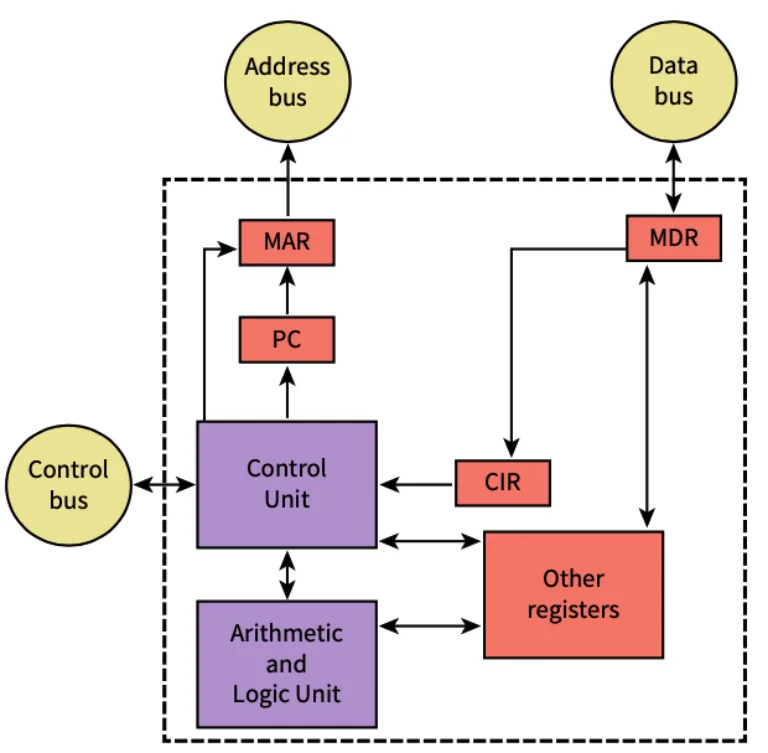
The stored program concept
- Program instructions and data are stored together in the same main memory.
- The processor fetches the instructions from memory one at a time and executes them in sequence.
Practise this: past-paper questions
4.1 · 2 of 30Book page Contents
The processor and the Arithmetic and Logic Unit (ALU)
The processor, or Central Processing Unit (CPU), is the hardware component inside the computer that executes the instructions of programs. It is made up of several important components, and each one has a specific role.
The Arithmetic and Logic Unit (ALU) carries out arithmetic calculations and logical operations, including:
- addition, subtraction, multiplication and division
- logical bitwise operations, such as AND, OR, NOT and XOR
- comparisons between values, such as greater than, less than and equal to
- shifting binary patterns to the left or right.
Practise this: past-paper questions
- June 2021 · Paper 12 · Q5(a)Complete the following descriptions of internal components of a computer by writing the missing terms. The transmits the signals to coordinate…
- November 2023 · Paper 13 · Q9(a)(i)Identify three other components in the Von Neumann model of a computer system. Do not include registers or buses in your answers
- June 2025 · Paper 12 · Q1(a)The table has six statements about the Von Neumann model for a computer system. Three of the statements are incorrect. Statement number |…
Used later in
4.1 · 3 of 30Book page Contents
The Control Unit (CU)
Builds on
The control unit (or program control unit) organises the order in which the program instructions are executed, and decodes each instruction. Decoding an instruction means the opcode and operand of the instruction are analysed to work out what must be done to execute it: what type of instruction it is and which addressing mode it uses, fetching any data it needs, and setting up the sequence of micro-operations. So the control unit directs the operations of all the other components of the processor.
Tasks of the control unit
- It sends control signals so that data can be read (loaded) from main memory and written (stored) to main memory.
- It decodes every instruction the processor will execute to work out what needs to be done (for example, an arithmetic calculation, a logic operation, a branch to another instruction, or loading or storing data in main memory).
- It organises the sequence of micro-operations needed to carry out an instruction.
- It sends control signals that decide which operation the ALU carries out each time.
Practise this: past-paper questions
- November 2022 · Paper 11 · Q5(b)(iii)Describe the purpose of the Control Unit (CU) in a CPU
- June 2023 · Paper 13 · Q7(b)The computer has a Control Unit (CU), system clock and control bus. Explain how the CU, system clock and control bus operate to transfer data…
- November 2023 · Paper 13 · Q9(a)(i)Identify three other components in the Von Neumann model of a computer system. Do not include registers or buses in your answers
- November 2024 · Paper 11 · Q3(a)State the purpose of the system clock and the Control Unit (CU) in a CPU. System clock CU
4.1 · 4 of 30Book page Contents
The system clock
The system clock (often just called the clock) produces regular clock pulses: a signal that keeps switching between a low state (0) and a high state (1). The clock signal is used to synchronise the operations of the components of the processor.
A rising edge is a change from low (0) to high (1). The opposite, a change from high to low, is a falling edge. The time between two rising edges, one after the other, is the clock period, and it is one clock cycle.
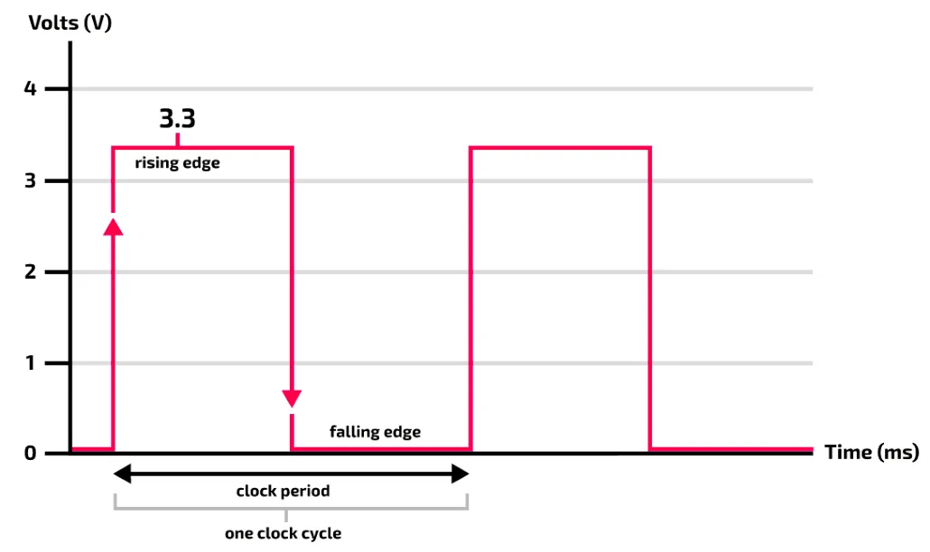
Each operation of the processor usually takes several clock cycles, and the number of cycles depends on the type of processor. For example, fetching data from memory can take many clock cycles even though it is described as one operation.
The clock speed (also called the clock rate or clock frequency) is the number of clock cycles that can be completed in one second. It is measured in hertz (Hz), usually megahertz (MHz) or gigahertz (GHz). It is the inverse of the clock period: clock frequency = 1 / clock period.
Practise this: past-paper questions
- June 2021 · Paper 12 · Q5(a)Complete the following descriptions of internal components of a computer by writing the missing terms. The transmits the signals to coordinate…
- November 2022 · Paper 13 · Q4(b)A computer system contains a system clock. Describe the purpose of the system clock
- June 2023 · Paper 13 · Q7(b)The computer has a Control Unit (CU), system clock and control bus. Explain how the CU, system clock and control bus operate to transfer data…
- November 2024 · Paper 11 · Q3(a)State the purpose of the system clock and the Control Unit (CU) in a CPU. System clock CU
4.1 · 5 of 30Book page Contents
Immediate Access Store (IAS)
Builds on
The Immediate Access Store (IAS) holds the data and programs that the processor (CPU) needs to access. The CPU copies data and programs from backing store into the IAS, where they are held temporarily, because reading from and writing to the IAS is much faster than reading from and writing to backing store. So any important data an application needs is held in the IAS for a while, to speed up operations.
Immediate Access Store
- The IAS is another name for primary memory, the main memory (RAM).
- The CPU can access it directly.
- It holds the data and instructions that are currently in use.
Practise this: past-paper questions
4.1 · 6 of 30Book page Contents
Registers: general-purpose and special-purpose
Builds on
Registers are memory locations inside the processor that can be accessed extremely quickly. Do not confuse registers with the addressable locations of main memory.
Going to main memory can slow down the execution of instructions, so the processor uses registers to store, and quickly reach, the results of operations. The ALU is connected to a set of general-purpose registers. These keep the results of intermediate calculations that are part of a larger calculation.
Special-purpose registers (also called dedicated registers) are registers in the processor that each have one specific purpose. The registers used in the fetch-execute cycle are special-purpose registers, because each one has its own role in each stage of the cycle.
Differences between general-purpose and special-purpose registers
- A general-purpose register can hold any data the program is working on, such as an intermediate result. A special-purpose register has one particular role, such as the PC, which only holds the address of the next instruction.
- Special-purpose registers hold the state of the program being run (for example, the address of the next instruction or the instruction being executed). General-purpose registers hold temporary data while operations are carried out.
- General-purpose registers can be used directly by the programmer, for example in assembly language. Many special-purpose registers are used only by the processor itself, for example during the fetch-execute cycle.
Practise this: past-paper questions
Used later in
4.1 · 7 of 30Book page Contents
The special-purpose registers
Builds on
These are the special-purpose registers you need to know, and the role of each one:
- Program Counter (PC): holds the address of the next instruction to be executed by the processor.
- Current Instruction Register (CIR): holds the instruction that the processor is executing now.
- Memory Address Register (MAR): temporarily holds the address of the location in main memory that the processor needs to access, either to read from it (load data) or to write to it (store data).
- Memory Data Register (MDR), also called the memory buffer register (MBR): temporarily holds the data (data values or instructions) that has been read from main memory or is about to be written to it.
- Accumulator (ACC): stores the result of a calculation carried out by the ALU. While a calculation is being worked out, the processor can keep temporary values in general-purpose registers, but the result ends up in the accumulator.
- Index Register (IX): used in indexed addressing in assembly language. The value it holds is added to the address given in an instruction to give the address that is actually used.
- Status Register (SR): stores information about the result of the last instruction the ALU executed. Each bit in the status register is a flag that shows whether an error or exception has happened, or that enables or disables interrupts.
The flags in the status register are used like this:
- An error or exception is when the result of a calculation needs further action. For example, a flag shows whether the result of a calculation is negative or zero, or whether the calculation produced an overflow or a carry.
- An interrupt is an event outside the running program that needs the attention of the processor, for example a hardware fault.
Practise this: past-paper questions
- November 2021 · Paper 12 · Q8(a)(i)Describe the role of the following special purpose registers in the fetch-execute (F-E) cycle. Memory Address Register (MAR) Memory Data Register…
- November 2021 · Paper 12 · Q8(a)(ii)Another special purpose register is the Index Register. Identify one other special purpose register used in the Von Neumann model for a computer…
- November 2022 · Paper 11 · Q5(b)(i)State the role of the following registers. Program Counter (PC) Index Register (IX) Status Register (SR)
- November 2022 · Paper 13 · Q4(a)(i)State the roles of the following registers. Memory Address Register (MAR) Memory Data Register (MDR)
Show 8 more
- November 2023 · Paper 11 · Q5(a)The Memory Data Register (MDR), Index Register (IX) and the Accumulator (ACC) are examples of special purpose registers. Identify two other…
- November 2024 · Paper 11 · Q8(a)Describe the purpose of the Status Register (SR)
- November 2024 · Paper 12 · Q3(a)The computer is designed using the Von Neumann model for a computer system. Complete the table by describing the purpose of each of the given…
- June 2025 · Paper 12 · Q1(a)The table has six statements about the Von Neumann model for a computer system. Three of the statements are incorrect. Statement number |…
- June 2025 · Paper 12 · Q1(b)Registers that are used in the Fetch-Execute (F-E) cycle include the PC, MAR, MDR and the ACC. Identify one other register and describe its role…
- November 2025 · Paper 11 · Q6(a)The processor uses several registers, including the Accumulator (ACC) and the Current Instruction Register (CIR). Complete the table by describing…
- November 2025 · Paper 12 · Q3(a)(ii)Registers such as the Accumulator (ACC) and the Index Register (IX) are used in the CPU. Identify two special purpose registers used in the CPU.…
- November 2025 · Paper 13 · Q6(b)The Von Neumann model for a computer system uses registers. Describe the role of the Memory Address Register (MAR) and Memory Data Register (MDR)…
Used later in
4.1 · 8 of 30Book pages Contents
Buses and the system bus
Builds on
The components of a computer system are connected together by buses. A bus is a communication system that transfers data between components.
- The system bus is a set of parallel connections that lets the internal components communicate with each other and exchange data.
- External buses connect peripherals to the processor. These can be serial or parallel connections.
Buses are made in different ways, depending on their use: for example wires, electronic pathways, and tracks on printed circuit boards.
In the Von Neumann architecture, the system bus is made up of an address bus, a data bus and a control bus. The system bus connects the processor (CPU), main memory and the I/O controllers, as this model shows:
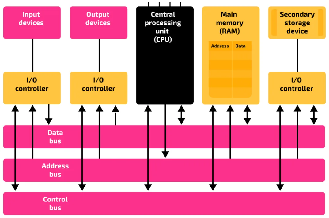
These points help you identify the components on a diagram that is unlabelled or only partly labelled:
- Input, output and secondary storage devices communicate with the internal components through I/O controllers.
- There is a one-way connection from the I/O controller of an input device to the data bus.
- There is a one-way connection from the data bus to the I/O controller of an output device.
- There is a two-way connection between the data bus and the I/O controller of a secondary storage device.
- There is a one-way connection from the processor to the address bus, because only the processor can send out addresses.
- There is a one-way connection from the address bus to all the other components: main memory and the I/O controllers.
- There is a two-way connection between main memory and the data bus, and a one-way connection from the address bus to main memory.
Note Each bus is a set of parallel lines, not a single line.
Practise this: past-paper questions
4.1 · 9 of 30Book page Contents
The data bus
The data bus carries data and instructions. It is bidirectional: it gives a two-way connection between the internal components, so values can be written to a location or read from it.
- Data is carried to and from the processor.
- Data is carried to and from main memory.
- Data is carried to and from the I/O controllers.
- Instructions are carried from main memory into the processor, to be decoded and executed.
The width of the data bus is its number of parallel lines. This decides how many bits can be transferred in one operation, for example in one go between memory and the processor. It is usually a multiple of a byte, such as 8, 16, 32 or 64 bits.
- If the data bus is 8 bits wide, 8 bits can be transferred at one time.
- If the data bus is 16 bits wide, 16 bits can be transferred at one time.
In general, if the data bus is n bits wide, n bits can be transferred at one time. The amount of data that can be fetched at one time affects the performance of the processor.
Practise this: past-paper questions
4.1 · 10 of 30Book page Contents
The address bus
The address bus carries the address of the memory location that data is to be read (loaded) from or written (stored) to.
There is a one-way connection from the processor to the address bus, and a one-way connection from the address bus to main memory and to the I/O controllers. This is because the address bus is unidirectional: it lets the processor pick out one addressable unit, either a memory location or an I/O controller.
The width of the address bus is its number of parallel lines. This decides how many bits can be used to make the address of a memory location, for example 16, 32 or 64 bits.
- If the address bus is 8 bits wide, there are 28 = 256 different numbers that can be used as memory addresses.
- If the address bus is 16 bits wide, there are 216 = 65,536 different numbers that can be used as memory addresses.
In general, if the address bus is n bits wide, there are 2n numbers that can be used to address memory locations. So the width of the address bus decides the largest number of memory locations that can be addressed, which is the largest memory capacity the computer system can have. This is called the address space, and it can affect the performance of the processor.
Practise this: past-paper questions
- November 2022 · Paper 11 · Q5(b)(ii)Tick (✓) one box in each row to identify the system bus used by each CPU component. | CPU component | Data bus | Address bus | Control bus | |…
- November 2023 · Paper 12 · Q8(c)(ii)Describe the roles of the address bus, the data bus and buffers in the process of writing data to the optical disc reader/writer
4.1 · 11 of 30Book page Contents
The control bus
Builds on
The control bus carries control signals that manage and coordinate the operations inside a computer system. This includes passing status signals between components, and carrying the clock signals needed to coordinate operations. For example, a control signal can be used to:
- request communication between two units
- acknowledge a request for communication
- say what type of data is being transferred on the other buses (data values, instructions or addresses)
- synchronise the communication between components, using the clock pulses.
The control bus is bidirectional: it has two-way connections to the components it connects.
Examples of control signals
- Memory read: puts the data from a memory location (whose address is on the address bus) onto the data bus.
- Memory write: stores the data on the data bus in a memory location (whose address is on the address bus).
- Bus request: shows that a component needs to use a bus.
- Bus grant: tells a component that it can now use the bus it asked for.
- Bus busy: shows that a bus cannot be used, because another component is using it.
- Interrupt request: shows that something, such as an error or exception, needs the attention of the processor (CPU).
- Clock signals: the control bus carries the clock pulses made by the system clock to the components.
How the control unit, system clock and control bus work together
- The system clock produces regular pulses that the control unit uses to time and synchronise its operations.
- The control unit sends control signals, such as memory read or memory write, along the control bus.
- The control bus also carries the clock signals, so every component works in step.
- The address goes on the address bus and the data then moves on the data bus.
Practise this: past-paper questions
- June 2021 · Paper 12 · Q5(a)Complete the following descriptions of internal components of a computer by writing the missing terms. The transmits the signals to coordinate…
- November 2022 · Paper 11 · Q5(b)(ii)Tick (✓) one box in each row to identify the system bus used by each CPU component. | CPU component | Data bus | Address bus | Control bus | |…
- June 2023 · Paper 12 · Q5(a)The laptop is designed using the Von Neumann model for a computer system. Identify two types of signal that a control bus can transfer
- June 2023 · Paper 13 · Q7(b)The computer has a Control Unit (CU), system clock and control bus. Explain how the CU, system clock and control bus operate to transfer data…
4.1 · 12 of 30Book pages Contents
The fetch-decode-execute cycle
Builds on
Every time the processor carries out an instruction, it goes through three main stages: it fetches the instruction, decodes it and executes it. Then it goes back to fetch the next instruction. These stages form the fetch-decode-execute cycle, also called the fetch-execute (F-E) cycle or the instruction cycle, because they are repeated for every instruction of every program that runs on the computer.
The cycle is used for both application software and system software. Behind everything you do on a computer (playing a game, filling in a spreadsheet, debugging a program, checking your emails) there are thousands of instructions, each carried out by going round the cycle.
Before the cycle can start, the program's instructions must be ready to be carried out. This means:
- the program instructions have been translated into machine code
- the program instructions have been loaded from secondary storage into main memory (RAM).
At the end of the cycle for each instruction, the processor checks the status register to see whether an error, an exception or an interrupt needs to be handled. For example, if an interrupt is shown, control may be passed to the matching interrupt service routine.
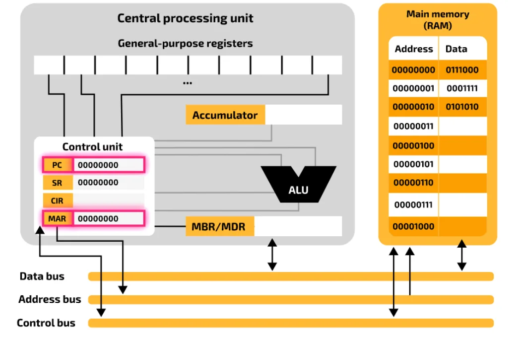
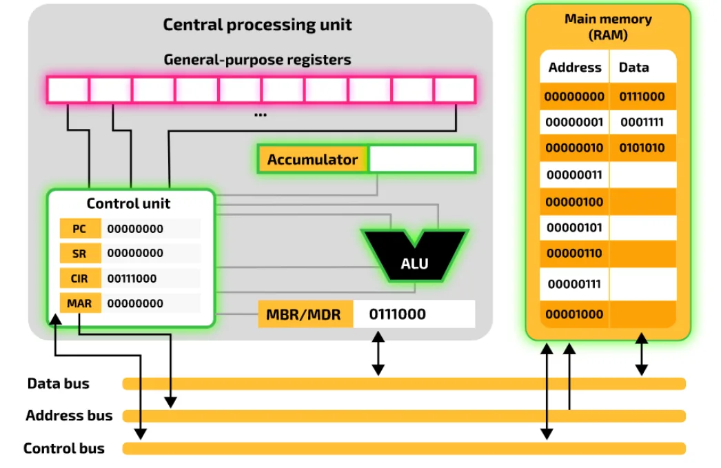
To see what happens at each stage, the next sections use this simplified model of a computer system, so you can focus on the important parts:
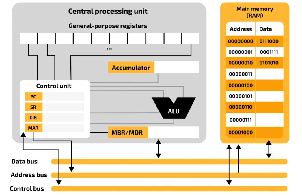
- All the components are connected to the control unit. This shows that the control unit sets up the paths that data takes between the internal components. For example, it sends values from general-purpose registers into the ALU, takes the output of the ALU, and saves it in the accumulator.
- The processor communicates with RAM through two special-purpose registers: the memory data register (also called the memory buffer register) and the memory address register. This does not mean that the general-purpose registers or the accumulator can never exchange data with main memory directly. That depends on the type of instruction being executed, and is also managed by the control unit.
Used later in
4.1 · 13 of 30Book pages Contents
The fetch stage
Builds on
To fetch an instruction from main memory:
- The program counter (PC) holds the address of the next instruction to be executed. The contents of the PC are copied to the memory address register (MAR), which is connected to the address bus. So the address of the next instruction is put on the address bus.
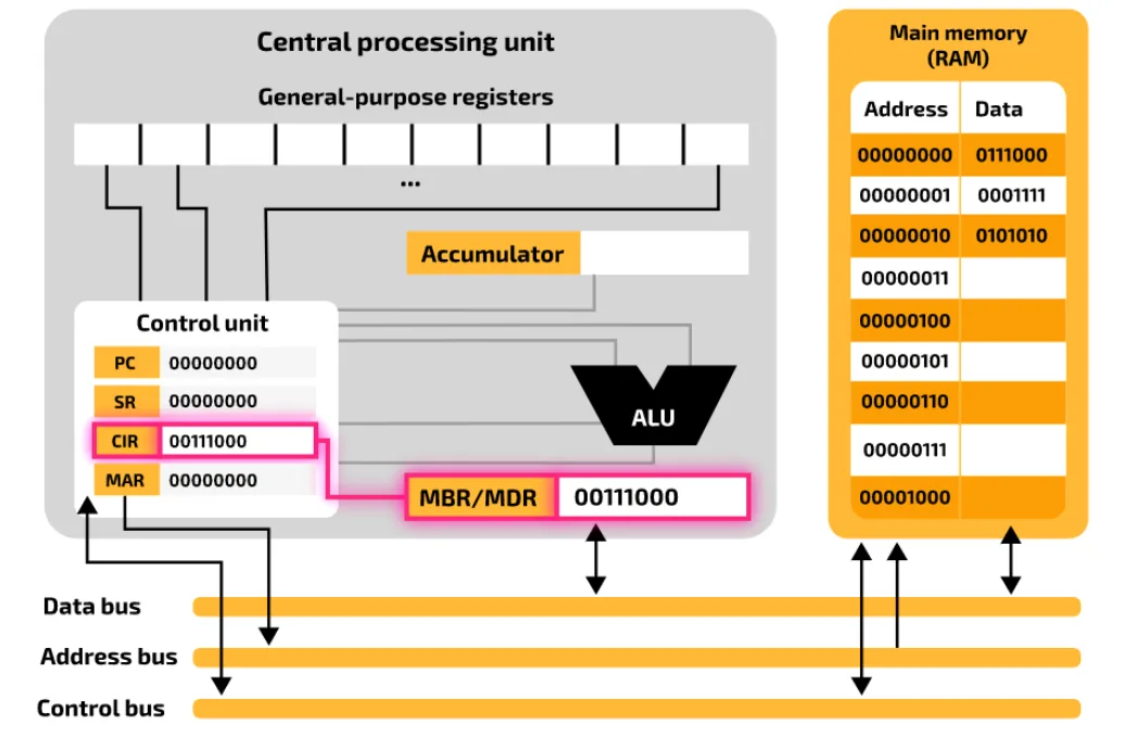
- Once the address is on the address bus, the control unit sends a memory read signal so that the contents of that memory location are sent to the processor. The instruction stored at that address is carried on the data bus from main memory to the processor, and saved in the memory data register (MDR), also called the memory buffer register (MBR). At the same time, the contents of the program counter (PC) are increased by one, so that it points to the address of the next instruction to fetch.
- The contents of the MDR are copied to the current instruction register (CIR). This keeps the current instruction safe, so the MDR is free to hold any extra data needed during the execute stage.
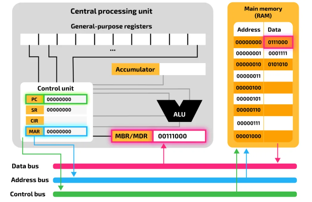
In a program that runs in sequence, the next instruction is normally in the next memory location. That is why the PC is increased by one. But if the next instruction is a branch to another place in the program, the PC is changed to point to the right address.
Practise this: past-paper questions
4.1 · 14 of 30Book page Contents
The decode stage
Builds on
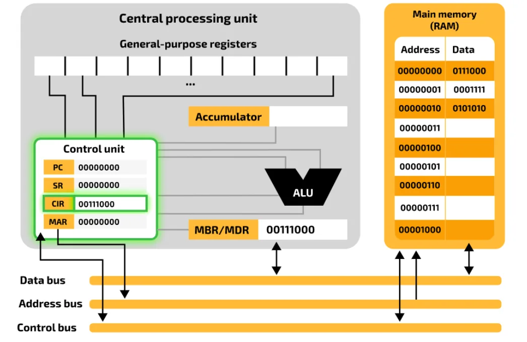
The control unit decodes the instruction held in the current instruction register (CIR). It splits the instruction into its opcode and operand, to work out what type of instruction must be carried out, whether more data is needed from memory, and where in main memory that data is stored.
Used later in
4.1 · 15 of 30Book page Contents
The execute stage
Builds on
The instruction is executed. The exact steps depend on the type of instruction. For example, for an arithmetic instruction such as adding two numbers, any data needed is fetched from main memory, the calculation is carried out by the Arithmetic and Logic Unit (ALU), and the result is stored in the accumulator, in a general-purpose register, or back in main memory.
If the program needs an instruction that is not the next one in sequence, for example because the current instruction is a branch, the address of the next instruction is worked out at this stage and loaded into the program counter (PC).
4.1 · 16 of 30Book page Contents
The role of the registers in the fetch-execute cycle
Builds on
Role of the registers in the fetch-execute cycle
- The Program Counter (PC) holds the address of the next instruction. Its contents are incremented, or changed, to the next address in each cycle.
- The Memory Address Register (MAR) holds the address to fetch the data from (copied from the PC).
- The Memory Data Register (MDR) holds the data at the address in the MAR.
- The instruction is transferred to the Current Instruction Register (CIR) to be decoded and executed.
Practise this: past-paper questions
- June 2021 · Paper 11 · Q3(a)Complete the following description of the role of the registers in the fetch-execute cycle by writing the missing registers. The holds the address…
- November 2021 · Paper 12 · Q8(a)(i)Describe the role of the following special purpose registers in the fetch-execute (F-E) cycle. Memory Address Register (MAR) Memory Data Register…
- June 2022 · Paper 11 · Q6(a)(i)Describe the role of the registers in the Fetch-Execute (F-E) cycle
- November 2022 · Paper 13 · Q4(a)(i)State the roles of the following registers. Memory Address Register (MAR) Memory Data Register (MDR)
Show 3 more
- November 2024 · Paper 12 · Q3(a)The computer is designed using the Von Neumann model for a computer system. Complete the table by describing the purpose of each of the given…
- June 2025 · Paper 12 · Q1(b)Registers that are used in the Fetch-Execute (F-E) cycle include the PC, MAR, MDR and the ACC. Identify one other register and describe its role…
- November 2025 · Paper 13 · Q6(b)The Von Neumann model for a computer system uses registers. Describe the role of the Memory Address Register (MAR) and Memory Data Register (MDR)…
4.1 · 17 of 30Book page Contents
Register transfer notation
Builds on
Operations that involve registers can be described in register transfer notation. Here is the fetch stage of the fetch-execute cycle written in register transfer notation:
| Register transfer notation | What it means |
|---|---|
MAR ← [PC] | The contents of the PC are copied into the MAR. |
PC ← [PC] + 1 | The PC is incremented by 1. |
MDR ← [[MAR]] | The data stored at the address held in the MAR is copied into the MDR. |
CIR ← [MDR] | The contents of the MDR are copied into the CIR. |
Each line is written like an assignment in a program:
- The first item, on the left, is where the data goes: the abbreviation of the register.
- The arrow shows the data being moved. To the right of the arrow is the data itself.
- Square brackets around a register mean the contents of that register are being moved. The move can include an arithmetic operation, such as + 1.
- Two transfers on the same line, separated by a semicolon, take place at the same time.
- The double brackets on the MDR line need care. The content of the MAR is an address, and it is the content of that address in memory that is copied into the MDR.
The PC is incremented at the same time as the memory read, so the middle two transfers are often written on one line:
MAR ← [PC]
PC ← [PC] + 1; MDR ← [[MAR]]
CIR ← [MDR]
Practise this: past-paper questions
- November 2021 · Paper 11 · Q6(a)There are two errors in the following register transfer notation for the fetch-execute cycle. 1 MAR ← [PC] 2 PC ← [PC] - 1 3 MDR ← [MAR] 4 CIR ←…
- June 2022 · Paper 13 · Q2(a)The Fetch-Execute (F-E) cycle is represented in register transfer notation. Describe each of the given steps. | Step | Description | | PC ← [PC] +…
- November 2022 · Paper 12 · Q7(c)Write the register transfer notation for each of the stages in the fetch-execute cycle described in the table. | Description | Register transfer…
- June 2023 · Paper 13 · Q7(c)Complete the table by writing the register transfer notation for each stage of the Fetch-Execute (F-E) cycle given in the table. Stage description…
Show 2 more
- November 2023 · Paper 13 · Q9(b)The following incomplete table contains steps of the Fetch-Execute (F-E) cycle and their descriptions. Complete the table by writing the missing…
- June 2025 · Paper 13 · Q2(a)(ii)The processor runs the Fetch-Execute (F-E) cycle. Write the stages of the F-E cycle using register transfer notation
4.1 · 18 of 30Book page Contents
Factors affecting processor performance
The performance of a computer's processor depends on several features. Most users want their computer to work faster, especially for processor-intensive tasks such as video editing, and manufacturers keep improving their processors so that they perform better than earlier versions. Knowing the key factors tells you when an upgrade might be needed. The factors are:
- processor type and the number of cores
- cache memory
- clock speed
- bus width: the width of the data bus and of the address bus.
Processor type: different types of processor are designed in different ways, so one type can do more work in each clock cycle than another. Two processors with the same clock speed and the same number of cores do not always perform the same.
Practise this: past-paper questions
- June 2022 · Paper 11 · Q6(b)Identify one factor that can affect the performance of the computer system and state how it impacts the performance. Factor Impact
- November 2022 · Paper 13 · Q4(c)Upgrading secondary storage to solid state typically improves the performance of computer systems. Identify one other upgrade to the hardware and…
- June 2023 · Paper 12 · Q5(b)Describe two ways the hardware of a laptop can be upgraded to improve the performance and explain how each upgrade improves the performance
- November 2024 · Paper 11 · Q3(b)(i)The number of cores in the processor affects the performance of the computer system. Identify one other feature of a processor that can affect the…
4.1 · 19 of 30Book page Contents
Multiple cores
A computer with more than one processing unit (core) is called multicore. For example:
- dual-core: two processing units
- quad-core: four processing units
- hexa-core: six processing units
- octo-core: eight processing units
In general, the more cores a computer has, the more instructions it can execute at the same time. So it performs better than a computer with the same type of processor but fewer cores.
But a quad-core processor does not process twice as many instructions in the same time as a dual-core processor running at the same speed. It is still a big improvement, but not double, because:
- data and instructions have to be passed to the cores in the right way, so the computer system has to spend time organising which cores receive which data and instructions
- the gain depends on the nature of the task: whether the work can be split into subtasks that are processed in parallel, one subtask per core at the same time. This is called parallel processing, and it needs more than one core (or processor).
For example, a task that needs four passes might be done in one pass on a quad-core processor, if the task can be split. If it cannot, the parts of the task sent to a particular core have to wait in a queue, which slows down completion. When the steps of a process must happen in a strict order, they may not be able to run in parallel until the queued steps have finished. Often, though, a task can be split into subtasks and the subtasks scheduled for processing. In general, a multicore system gives the chance to complete instructions faster than a system with fewer cores, and many programs are now written to make the most of parallel processing.
Practise this: past-paper questions
- June 2021 · Paper 12 · Q5(b)Describe the ways in which the following factors can affect the performance of his laptop computer. Number of cores Clock speed
- November 2023 · Paper 11 · Q5(c)(ii)A second computer has a CPU with two 2.1 GHz cores. Explain why the second computer does not always run twice as fast as the computer with one 2.1…
- November 2025 · Paper 11 · Q6(b)Increasing the number of cores in a processor can affect the performance of a computer. Describe the drawbacks of increasing the number of cores…
4.1 · 20 of 30Book pages Contents
Cache memory
Builds on
A cache is a fast, fairly small set of memory locations close to the processor. It stores the instructions and data that are used most often.
While programs run, a computer system keeps moving data in and out of cache and RAM. When an instruction, or a set of instructions, is used again and again, fetching it from RAM each time is slow. So cache memory is used to store the instructions that are likely to be needed. Like RAM, cache memory is erased when the power is switched off.
The size of cache memory varies a lot between older and newer systems. Cache is now measured in megabytes, far smaller than RAM (usually measured in gigabytes), because cache memory is expensive compared with RAM. Unlike RAM, cache memory cannot easily be upgraded or replaced.
Most modern computer systems have three levels of cache, and some now have a fourth. Data and instructions are passed along from the slowest cache (L3 or L4) to the fastest (L1):
- Level 1: L1 cache is part of the circuitry of each core. It is the smallest and fastest cache. A quad-core CPU has four L1 caches.
- Level 2: L2 cache is often shared by cores. It is slower than L1 cache and usually larger. In new systems, the L2 cache is usually part of each core, like the L1 cache.
- Level 3: L3 cache is slower than L2 cache but larger. It is on the processor or near it on the motherboard.
- Level 4: newer systems have an L4 cache. Like L3, it is on or near the processor.
How cache memory improves performance
- Cache memory is faster to access than RAM, so instructions and data held in cache reach the processor more quickly.
- The larger the cache, the more instructions and data can be held ready to be carried out, so the processor has to go to main memory less often.
- Without cache, the processor must access main memory more often, which makes each operation take longer.
- The faster the cache, the faster an instruction is fetched to the processor.
- Where the cache is placed also matters: L2 cache inside each core cuts the time instructions and data take to reach the core's registers.
- More levels of cache make the system more efficient, as more data is held closer to the CPU.
Practise this: past-paper questions
- November 2022 · Paper 11 · Q7(d)Explain the reasons why increasing the amount of cache memory can improve the performance of a CPU
- June 2025 · Paper 13 · Q2(b)The computer has cache memory. Describe one benefit of the computer using cache memory
- November 2025 · Paper 12 · Q3(c)A student buys a new computer. The table shows the specifications of the old computer and the new computer. Old computer | New computer 1.8 GHz…
4.1 · 21 of 30Book page Contents
Clock speed
Processors are measured by their clock speed. The clock is an electronic oscillator that produces a signal to synchronise the operations of the processor. In general, the higher the clock speed, the faster instructions are carried out. Clock speed is usually measured in gigahertz (GHz).
For example, an i9 multicore processor with a clock speed of 3.6 GHz can make 3.6 billion clock cycles (state changes) per second. But one instruction usually takes more than one clock cycle, so a 3.6 GHz processor does not process 3.6 billion instructions per second. Clock speed is a theoretical maximum, and a system is unlikely to reach it.
Making a processor run more cycles per second than it is designed for is called overclocking. It can make the processor overheat.
Practise this: past-paper questions
- June 2021 · Paper 12 · Q5(b)Describe the ways in which the following factors can affect the performance of his laptop computer. Number of cores Clock speed
- November 2023 · Paper 11 · Q5(c)(i)Describe how increasing the clock speed to 4 GHz can increase the performance of the computer
- November 2025 · Paper 12 · Q3(c)A student buys a new computer. The table shows the specifications of the old computer and the new computer. Old computer | New computer 1.8 GHz…
4.1 · 22 of 30Book pages Contents
Data bus width
The width of the data bus decides how many bits can be transferred in one operation (at the same time, in one go). The wider the data bus, the better the processor performs, because more data can be transferred between the internal components at the same time.
If the data bus is n bits wide, n bits can be transferred between the internal components in one operation:
- an 8-bit data bus transfers 8 bits (1 byte) at a time
- a 16-bit data bus transfers 16 bits (2 bytes) at a time.
The wider the bus, the larger the piece of data or instruction that can be transferred between main memory and the processor in one go. So, if everything else stays the same, a wider data bus passes more data at a time and cuts the time it takes for data and instructions to be processed.
A wider data bus also lets larger values be sent between the internal components. If a bit pattern stands for a number and the data bus is n bits wide, then 2n different values can be sent in one go, so the largest is 2n − 1. For example:
- with an 8-bit data bus, a number sent in one go has up to 8 bits, so its largest value is 28 − 1 = 255
- with a 16-bit data bus, a number sent in one go has up to 16 bits, so its largest value is 216 − 1 = 65,535.
Think of a computer system with an 8-bit data bus that has to process a number that needs 16 bits (any number greater than 255). It has to fetch from main memory twice. The first fetch brings 8 bits of the number, and the second fetch brings the other 8 bits, which are joined to the first 8 in a larger register. A 16-bit system can do this in one fetch, which makes the processor perform much better, as there are fewer delays when fetching data.
This is why most computer systems have a data bus width equal to the word length of the system: if a computer uses a 16-bit word, the data bus is 16 bits wide. Then the contents of each addressable memory location can be sent in one go.
4.1 · 23 of 30Book page Contents
Address bus width and the amount of RAM
Builds on
The width of the address bus decides how many bits can be used to make the address of a memory location. The wider the address bus, the more memory locations can be addressed. So the processor can use a larger main memory for data and instructions, which also improves performance because it relies less on slower virtual memory.
If the address bus is n bits wide, there are 2n addresses available for main memory, so the processor can reach 2n different memory locations. For example:
- an 8-bit address bus gives 28 = 256 memory locations the processor can access
- a 16-bit address bus gives 216 = 65,536 memory locations the processor can access.
Performance improves because, with more memory, the data and instructions to be processed do not have to be fetched from secondary storage, which is much slower.
A wider address bus only improves performance if the instructions and data cannot all be held in main memory. If they can, a larger address range does not help. But most modern multitasking systems use paging, and more main memory means less movement of data between main memory and secondary storage (HDD or SSD). Cutting down paging is an important way to make the computer visibly faster.
The amount of RAM and performance
- More RAM means more of the data and instructions in use can be held in main memory at once.
- So less data has to be fetched from (or swapped to) secondary storage, which is much slower.
- If a computer slows down, close applications you do not need, to free space in RAM. If it is still slow, upgrading the RAM is usually a good first step.
Practise this: past-paper questions
- November 2022 · Paper 13 · Q4(c)Upgrading secondary storage to solid state typically improves the performance of computer systems. Identify one other upgrade to the hardware and…
- June 2023 · Paper 12 · Q5(b)Describe two ways the hardware of a laptop can be upgraded to improve the performance and explain how each upgrade improves the performance
- June 2025 · Paper 11 · Q6(a)(ii)The two computers have different amounts of RAM. Explain how different amounts of RAM affect the performance of a computer
- June 2025 · Paper 11 · Q6(a)(iii)The two computers have different bus widths. Explain how different bus widths affect the performance of a computer
4.1 · 24 of 30Book page Contents
USB ports
The Universal Serial Bus (USB) is an asynchronous serial method of sending data. It has quickly become the standard way to transfer data between a computer and many kinds of device.
A USB cable is a shielded cable with four wires: two for power and earth, and two used to send data. When a device is plugged into one of the computer's USB ports:
- the computer automatically detects that a device is there (because of a small change in the voltage on the data wires in the cable)
- the device is automatically recognised, and the right device driver is loaded so that the computer and the device can communicate
- if the device is new, the computer looks for a device driver that matches it. If none is available, the user is asked to download the right software.
Practise this: past-paper questions
- June 2023 · Paper 12 · Q5(c)(i)A printer is connected to a Universal Serial Bus (USB) port. Describe how data is transmitted through a USB port
- November 2024 · Paper 11 · Q3(b)(ii)A solid state (flash) memory drive is automatically recognised by the computer when it is plugged into a port in the computer. Identify an…
4.1 · 25 of 30Book pages Contents
VGA and HDMI ports
Builds on
Video Graphics Array (VGA) was introduced at the end of the 1980s. It is an analogue system. VGA supports a resolution of 640 × 480 pixels on a television or monitor screen, with a refresh rate of up to 60 Hz (60 frames a second), as long as only 16 different colours are used. If the resolution is reduced to 320 × 200, it can show up to 256 colours.
High-Definition Multimedia Interface (HDMI) ports send both audio and video output from a computer to an HDMI-enabled device. They support high-definition signals. HDMI was introduced as a digital replacement for the older analogue VGA system. Modern high-definition (HD) televisions have these features, which are making VGA out of date:
- a widescreen format (16:9 aspect ratio)
- more pixels on the screen (typically 1920 × 1080)
- a faster refresh rate (such as 120 Hz, or 120 frames a second)
- a very large range of colours (some companies claim up to four million).
So modern HD televisions need much more data, received at a much faster rate than older televisions (around 10 gigabits per second). HDMI has a higher bandwidth, so it can supply the data needed for high-quality sound and pictures.
HDMI also gives some protection against piracy, because it uses high-bandwidth digital copy protection (HDCP). HDCP uses a type of authentication protocol. For example, a Blu-ray player checks the authentication key of the device it is sending data to (such as an HD television). If the key is authenticated, handshaking takes place and the Blu-ray player starts sending data to the device.
| VGA | HDMI | |
|---|---|---|
| Signal | Analogue | Digital |
| What it carries | Video only, no sound | Video and audio in one cable |
| Resolution and colours | Low resolution and few colours | High-definition resolutions, many more colours |
| Bandwidth | Lower | Higher, so more data per second |
| Copy protection | None | HDCP |
Practise this: past-paper questions
- June 2023 · Paper 12 · Q5(c)(ii)A monitor is connected to the laptop using a different type of port. Identify one other type of port that can be used to connect the monitor
- November 2024 · Paper 12 · Q3(b)The student needs to connect the computer to a monitor that has a screen resolution of 2560 × 1600 pixels. The monitor also has built-in speakers.…
- June 2025 · Paper 13 · Q2(c)The computer connects to a monitor using a High Definition Multimedia Interface (HDMI) cable that connects into an HDMI port. Explain how HDMI…
4.1 · 26 of 30Book page Contents
Allocating processor time
Normally, the operating system (OS) divides processing time between the processes that are running. Time is shared between tasks depending on things such as:
- when the task was requested
- how important the task is
- how long the task is.
The more processes a computer is running, the longer a process may have to wait to be given processing time.
This way of sharing time does not work for processes that must do something almost immediately. For example, when a user presses a key to type a word into a word processor, the character should appear on the screen almost at once. If that process had to wait until all the other processes had finished, the user would notice the delay and typing would become uncomfortable.
The OS could give the keyboard-reading process more processing time. But then the processor might spend longer on keyboard reading than it needs to, leaving less time for other tasks, and the whole system would slow down.
4.1 · 27 of 30Book page Contents
Interrupts and their causes
Instead, devices use interrupts to get processing time for urgent work. An interrupt is a signal sent to the processor to ask for its immediate attention. When the processor receives this request, it stops what it is doing and runs the process linked to the interrupt.
Causes of interrupts
- A hardware device has signalled that it has data to process.
- A hardware device has finished a task it was asked to do.
- A software process needs a service, or an OS function to be carried out.
- A set amount of time has run out and an action needs to be taken.
- A hardware failure has happened and needs to be dealt with.
Practise this: past-paper questions
Used later in
4.1 · 28 of 30Contents
Hardware and software interrupts
Builds on
Interrupts can come from hardware devices or from software.
| Examples | |
|---|---|
| Hardware interrupt (from a device) | A key is pressed on the keyboard, the mouse is moved, the printer is out of paper, a device has finished sending or receiving data, power failure, a hardware fault |
| Software interrupt (from a program) | Division by zero (or another run-time error), stack overflow, a buffer is full, trying to use an invalid memory location (for example an array index out of range), two processes trying to use the same memory location, a program asking the operating system for a service |
| Timer interrupt (from the clock) | The time given to a process has run out, so the OS can give the processor to another process |
Note Take care with a full buffer: Cambridge counts “buffer full” as a software interrupt, not a hardware one, because the buffer is an area of memory that software manages.
Uses of interrupts include reading keyboard input as soon as a key is pressed, telling the processor that a printer has finished or needs attention, sharing processor time between programs, and stopping a program safely when it causes an error.
Practise this: past-paper questions
- November 2021 · Paper 12 · Q7(a)The Operating System handles interrupts. Tick (✓) one box in each row to identify whether each event is an example of a hardware interrupt or a…
- November 2022 · Paper 11 · Q5(d)Identify two causes of a software interrupt. 1 2
- November 2023 · Paper 13 · Q9(c)Interrupts can be caused by software programs or hardware devices. State one cause of a software interrupt
4.1 · 29 of 30Book page Contents
Interrupt service routines (ISR)
The operating system has interrupt service routines (ISRs), also called interrupt handlers, to deal with each type of interrupt. An ISR is a small program written to respond to the request an interrupt makes. ISRs can be part of the operating system, or provided by device drivers.
When a key is pressed, the ISR finds out which key it was by polling the keyboard, then stores that character in the keyboard buffer. A process that is waiting for keyboard input can later check the keyboard buffer to find out which key was pressed.
Practise this: past-paper questions
4.1 · 30 of 30Book pages Contents
Servicing an interrupt in the fetch-execute cycle
Builds on
If there are no interrupts, the processor repeats the fetch-decode-execute cycle, executing the instructions of the running process one after another. An interrupt makes the processor stop what it is executing so it can run the ISR. When the ISR has finished, the processor must go back to the instruction it was executing before the interrupt and carry on from where it left off.
In general, an interrupt affects the fetch-decode-execute cycle of a running program like this:
- The processor receives the interrupt.
- The processor finishes the fetch-decode-execute cycle of the instruction it was running when the interrupt arrived.
- The current contents of the processor registers (including the program counter) are saved to memory.
- The source of the interrupt is found, so that the right ISR is called.
- All other interrupts of lower priority are put on hold, so that the ISR can finish running.
- The program counter is loaded with the address of the first instruction of the ISR.
- The ISR runs until it is complete.
- The processor registers are reloaded with the values that were saved to memory.
- The lower-priority interrupts that were put on hold are allowed again.
- The program counter points to the address of the next instruction of the program that was running when the interrupt arrived.
Interrupt handling in the fetch-execute cycle
- Interrupts are detected at the end (or start) of each F-E cycle, when the processor checks whether an interrupt flag is set.
- The priority of the interrupt is checked.
- If its priority is lower than the current process, the F-E cycle carries on.
- If its priority is higher, the state of the current process (the contents of the registers) is saved on the stack.
- The source or type of the interrupt is identified, and the right ISR is called to handle it.
- When the ISR has finished, the processor checks for further interrupts of high priority, and handles them in the same way.
- Otherwise, the saved values are loaded back from the stack and the process carries on.
Practise this: past-paper questions
- June 2022 · Paper 11 · Q6(a)(ii)Describe when interrupts are detected in the F-E cycle and how the interrupts are handled. Detected Handled
- June 2022 · Paper 13 · Q2(b)Explain how interrupts are handled during the F-E cycle
- November 2022 · Paper 13 · Q4(a)(ii)State when interrupts are detected during the Fetch-Execute (F-E) cycle
- June 2023 · Paper 11 · Q6An interrupt is generated when a key is pressed on a computer keyboard. Explain how the computer handles this interrupt
Show 2 more
4.1
Concepts in 4.1
Every idea explained in 4.1, and where else in the notes it is used.
Zain Merchant's notes, page by page, as printed in his book. The Notes tab has the same notes as text, with links.
Past-paper questions and mark schemes © Cambridge University Press & Assessment. Compiled for revision by Zain Merchant.
- June 2021 · Paper 11 · Q3Notes:The fetch stageThe role of the registers in the fetch-execute cycle
- June 2021 · Paper 12 · Q5Notes:The processor and the Arithmetic and Logic Unit (ALU)The system clockBuses and the system busThe control busMultiple coresClock speed
- November 2021 · Paper 11 · Q6Notes:Register transfer notation
- November 2021 · Paper 12 · Q7Notes:Hardware and software interrupts
- November 2021 · Paper 12 · Q8Notes:The special-purpose registersThe role of the registers in the fetch-execute cycle
- June 2022 · Paper 11 · Q6Notes:The fetch stageThe role of the registers in the fetch-execute cycleFactors affecting processor performanceServicing an interrupt in the fetch-execute cycle
- June 2022 · Paper 13 · Q2Notes:Register transfer notationServicing an interrupt in the fetch-execute cycle
- November 2022 · Paper 11 · Q5Notes:Computer architecture and the Von Neumann modelThe Control Unit (CU)The special-purpose registersThe address busThe control busInterrupts and their causesHardware and software interrupts
- November 2022 · Paper 11 · Q7Notes:Cache memory
- November 2022 · Paper 12 · Q7Notes:Register transfer notation
- November 2022 · Paper 13 · Q4Notes:The system clockThe special-purpose registersThe role of the registers in the fetch-execute cycleFactors affecting processor performanceAddress bus width and the amount of RAMServicing an interrupt in the fetch-execute cycle
- June 2023 · Paper 11 · Q6Notes:Interrupt service routines (ISR)Servicing an interrupt in the fetch-execute cycle
- June 2023 · Paper 12 · Q5Notes:The control busFactors affecting processor performanceAddress bus width and the amount of RAMUSB portsVGA and HDMI ports
- June 2023 · Paper 13 · Q7Notes:The Control Unit (CU)The system clockThe control busRegister transfer notation
- November 2023 · Paper 11 · Q5Notes:Immediate Access Store (IAS)The special-purpose registersMultiple coresClock speed
- November 2023 · Paper 12 · Q8Notes:The data busThe address bus
- November 2023 · Paper 13 · Q9Notes:Computer architecture and the Von Neumann modelThe processor and the Arithmetic and Logic Unit (ALU)The Control Unit (CU)Registers: general-purpose and special-purposeRegister transfer notationHardware and software interruptsServicing an interrupt in the fetch-execute cycle
- November 2024 · Paper 11 · Q3Notes:The Control Unit (CU)The system clockFactors affecting processor performanceUSB ports
- November 2024 · Paper 11 · Q8Notes:Registers: general-purpose and special-purposeThe special-purpose registers
- November 2024 · Paper 12 · Q3Notes:The special-purpose registersThe role of the registers in the fetch-execute cycleVGA and HDMI ports
- June 2025 · Paper 11 · Q6Notes:Data bus widthAddress bus width and the amount of RAM
- June 2025 · Paper 12 · Q1Notes:The processor and the Arithmetic and Logic Unit (ALU)The Control Unit (CU)The special-purpose registersThe role of the registers in the fetch-execute cycleServicing an interrupt in the fetch-execute cycle
- June 2025 · Paper 13 · Q2Notes:The Control Unit (CU)The system clockThe control busRegister transfer notationCache memoryVGA and HDMI ports
- November 2025 · Paper 11 · Q6Notes:The special-purpose registersMultiple cores
- November 2025 · Paper 12 · Q3Notes:The special-purpose registersCache memoryClock speed
- November 2025 · Paper 13 · Q6Notes:The special-purpose registersThe role of the registers in the fetch-execute cycle
Past-paper questions and mark schemes © Cambridge University Press & Assessment. Compiled for revision by Zain Merchant.
Try the questions first.
Write your answers, then check them against the mark scheme. Your choice is remembered on this device.